


Our official Samsung Galaxy S8 Review is out and now we want to know what’s inside the device. For the teardown treatment, IFIXIT worked on a Galaxy S8+. We’re really curious to know how both the Galaxy S8 and S8+ will fare against its main rival, the LG G6. We have our personal take but we’re looking forward how the whole Android community will see and experience the South Korean tech giant’s latest premium flagship device.
Samsung made us wait for another month as it skipped the Mobile World Congress. It’s understandable since the Note 7 debacle was really something to be bummed about but the company is now ready to take back what it lost last year. We’re feeling positive about the S8 duo because we know Samsung has done everything in its power. We’re banking on the improved quality assurance tests and standard protocols.
We have an idea about the phone on the surface but what about inside it? We want to know if it’s easy to open and repair as knowing such details allow us to make informed decisions whether the new smartphone is worth upgrading to.
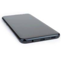
IFIXIT opened a Galaxy S8+ equipped with a 6.2-inch dual-edge Super AMOLED screen with 2960 × 1440 resolution, powered by a Qualcomm Snapdragon 835 and 4GB RAM, has a 64GB onboard storage, IP68-certified (water-resistant), and Android 7.0 Nougat-loaded. Its fingerprint sensor is found on the rear now, making the front side almost “feature-less” as the physical home button has been replaced by a sensor embedded under the display.
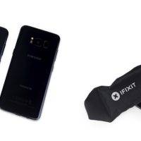
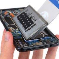
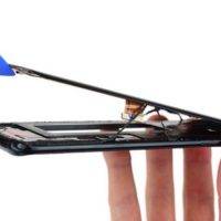
Using an iOpener, IFixit applied heat first to soften the sides of the Galaxy S8+. The rear glass was easily removed up so getting inside was easy. True enough, the fingerprint reader is found in the rear panel. It is tied to the motherboard with a short cable so it’s probably less prone to damage.
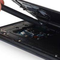
The Galaxy S8+ and Galaxy S8 are more similar to the old Galaxy S8 when we’re talking abot the rear glass panel. It may not be as durable as the S7 but this one looks easy to repair at least. IFixit tried to disconnect the battery but a connector is under the midframe. You’ll see nearby the upper antenna is the NFC-wireless charging panel that makes Samsung Pay possible.
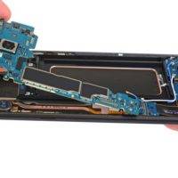
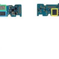
Trying to remove the battery again was a bit difficult because of the adhesive. And then the cameras and the motherboard are removed, followed by an iris scanning camera and front-facing camera. Checking the motherboard’s silicon closely, here’s what IFixit discovered
FRONT:
• Samsung K3UH5H50MM-NGCJ 4 GB LPDDR4 RAM layered over the MSM8998 Snapdragon 835
• Toshiba THGAF4G9N4LBAIR 64 GB UFS (NAND flash + controller)
• Qualcomm Aqstic WCD9341 audio codec
• Skyworks 78160-11
• Avago AFEM-9066
BACK:
• Qualcomm WTR5975 RF transceiver
• Murata KM7118064 Wi-Fi module
• Avago AFEM-9053
• Qualcomm PM8998 (similar to PM8920)
• NXP 80T71 NFC controller
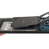
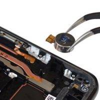
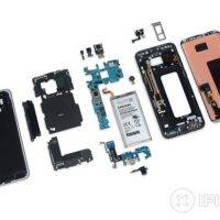
Prying open the phone further, there’s the speaker grille, USB Type-C connector, and a headphone jack. Setting aside the heat pipe and contact pad button cables, there’s the vibrator motor, sensor array, what looks like an RGB LED, IR emitter, and IR camera.
So is the Samsung Galaxy S8+ repairable? The IFixit guys only gave it a 4/10 score. Phone appears to be modular inside which means components, including the battery, can be replaced independently. The glass back and front panels appear to be “crackable” but tough to remove because of the strong adhesive. Even the curved screen looks difficult to remove.

VIA: IFIXIT


Hi guys, Is a chip (Snapdragon 835) available for buying (from you)? Thx