The race for developing stellar image sensors for phones has been going on for long now. Brands like Samsung, Apple, OPPO, Vivo, and Xiaomi have invested a lot in R&D for constantly improving the CMOS image sensors that are used on modern-day devices. Take for example the optical image stabilization, pixel binning tech or the telephoto lenses that at most times match an entry-level DSLR shooter. Now, Sony has taken the big leap in image sensor technology with its announcement at the IEEE International Electron Devices Meeting. The revelation details about the CMOS image sensor having a dual-layer Transistor Pixel for next-level photography on phones.
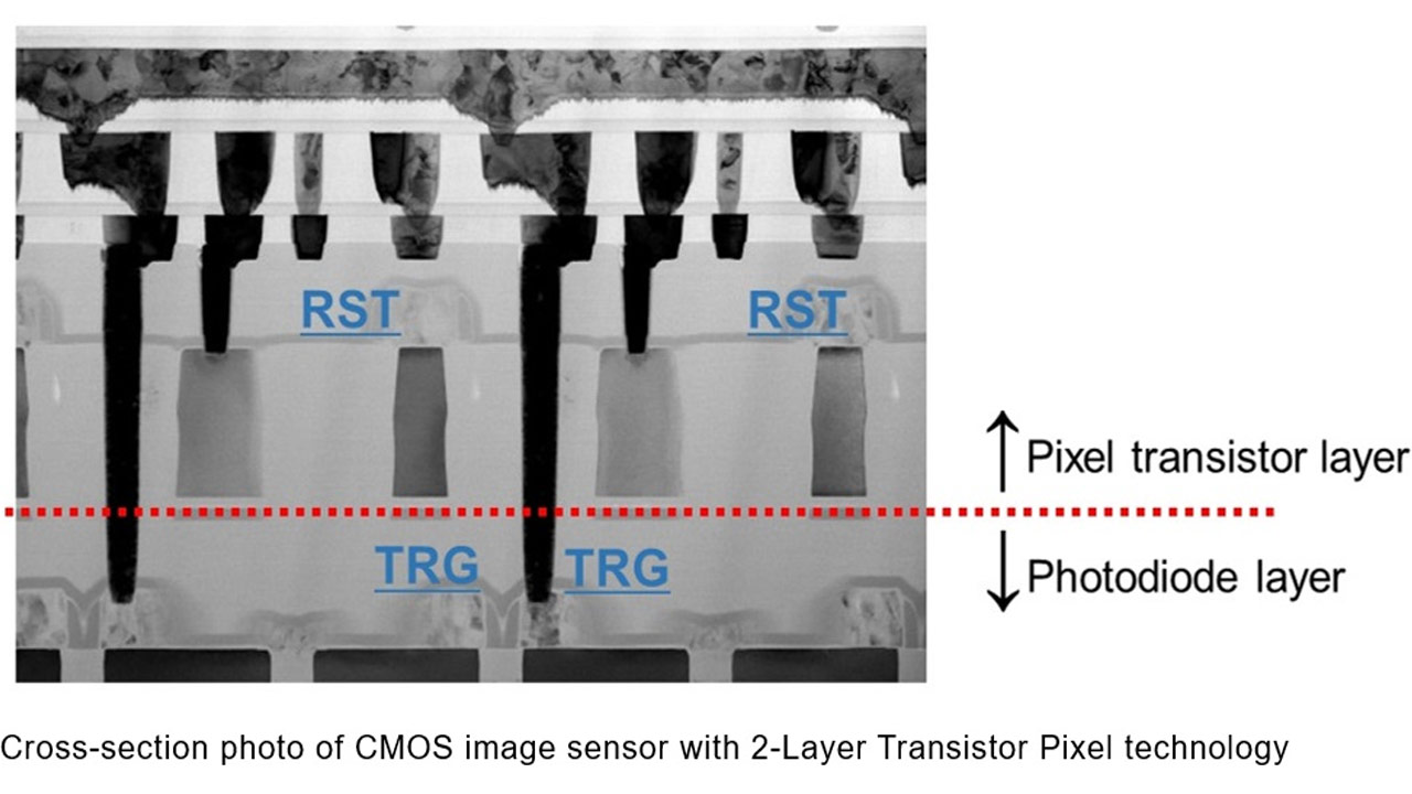
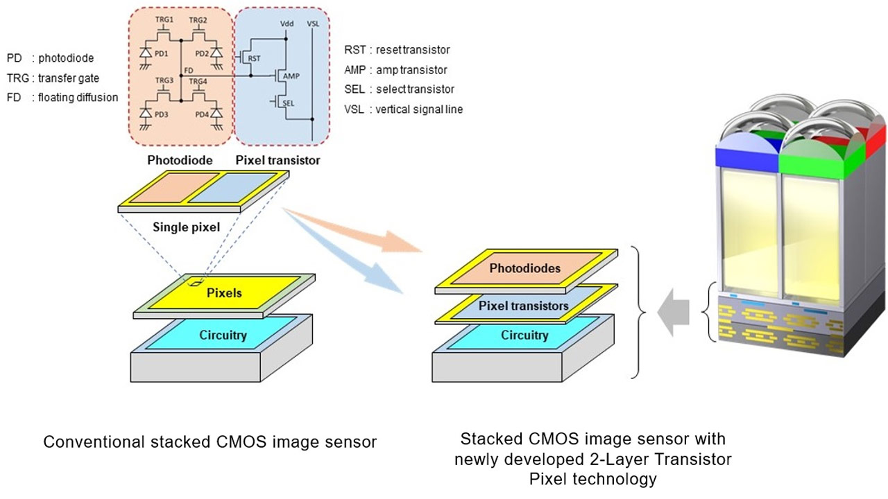
The technology employed here by Sony Semiconductor Solutions is the world’s first stacked image sensor that promises a wider dynamic range and excellent noise reduction. As compared to the conventional CMOS image sensors, this one has separate photodiodes and pixel transistors, set up on different substrate layers.

The stacked structure has a pixel chip having back-illuminated pixels on top of a logic chip. The photodiodes for converting light to electrical signals and the pixel transistors that control the signals are located side by side on the same layer.
This architecture, therefore, doubles the saturation signal level for improved image properties and good dynamic range. The amp transistors can be increased in size since there are two separate layers – also the transfer gates (TRG) including the reset transistors (RST) and select transistors (SEL) occupy a photodiode-free layer. Thus, resulting in better nighttime photography and reduced noise reduction in the darker locations.

According to Sony, the widened dynamic range, color correction, and excellent noise reduction will also help in eliminating chances of overexposure and underexposure while clicking pictures. The Tokyo-based electronics giant is planning to bring the 2-Layer Transistor Pixel technology to mobile devices in the near future.


