Are you familiar with Moore’s Law? It’s a trend described by Gordon E. Moore, co-founder of Intel, noting that the number of transistors that can be placed inexpensively on an integrated circuit doubles approximately every two years. What’s that got to do with Android? It’s quite simple – bigger processing power in the same size package. Today Intel has announced its 22nm 3D Tri-Gate transistors, processing technology that they say will bring 50% power reduction at constant performance (that means better battery life) and 37% performance increase at low voltage – a better job for less!
So what is 22nm – what’s that mean? “nm” stands for nanometer, one nanometer is equal to one billionth of a meter. In the semiconductor industry, this unit is used to describe the wavelength of light. All you and I really need to know is that this is the newest, the best, where back in 1989 we were at 800nm, 2002 we were at 90nm, and now we’re all the way down to 22nm. Again, this follows the plan – Intel had their OG Gordon Moore send out a quote on the matter:
“For years we have seen limits to how small transistors can get. This change in the basic structure is a truly revolutionary approach, and one that should allow Moore’s Law, and the historic pace of innovation, to continue”

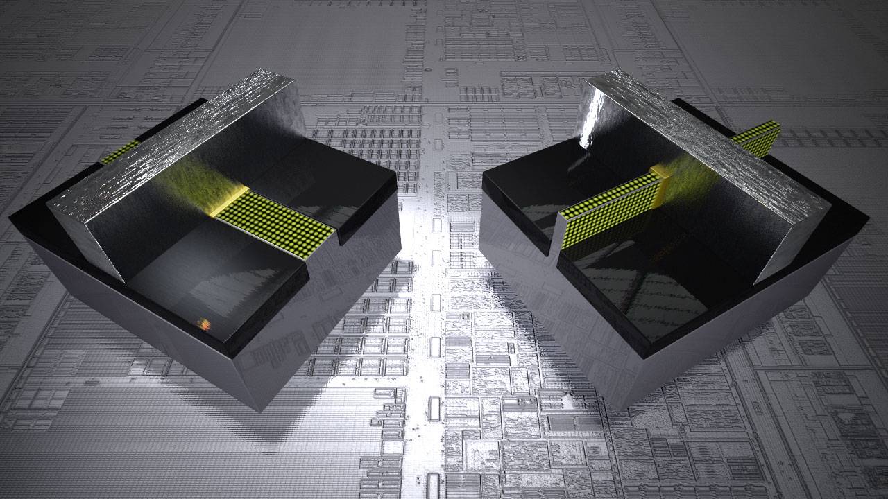
Next, what does “3D” stand for here? Hint – there’s no double camera tricky business going on here. It’s got to do with the structure of the transistor. The 3D Tri-Gate transistors form conducting channels on three sides of a vertical fin structure. This build results in less heat transmission, longer battery life in mobile devices, and because of a combo of the high-k gate insulators and strained silicon, improved performance.
Intel notes the following to confuse and excite you:
Tri-gate fully-depleted substrate transistors have a raised plateau-like gate structure with two vertical walls and a horizontal wall of gate electrode. This three-dimensional structure improves the drive current while the depleted substrate reduces the leakage current when the transistor is in the “off” state. Reducing leakage current not only helps control heat at the circuit level but also translates to increased battery life in mobile devices.
You can expect some other bits that you may or may not be super excited about from an Android standpoint: native PCIe 3.0 and USB 3.0 controllers at the processor level as well as an integrated DirectX graphics core with support for the second-generation of QuickSync. QuickSync is Intel’s media encoding/decoding acceleration technology, in case you do not know.

The first application of this technology will be in Intel’s Ivy Bridge processors, demonstrated today on some high-volume CPU’s, as noted by our sister site SlashGear. Have a peek at some videos while we’re at it and see where Intel is at with the project at the moment:
https://www.youtube.com/watch?v=SB706hhCDZc
https://www.youtube.com/watch?v=rHeJezOLvEI
Press Release:
Intel Reinvents Transistors Using New 3-D Structure
New Transistors for 22 Nanometer Chips Have an Unprecedented Combination of Power Savings and Performance Gains
NEWS HIGHLIGHTS
Intel announces a major technical breakthrough and historic innovation in microprocessors: the world’s first 3-D transistors, called Tri-Gate, in a production technology.
The transition to 3-D Tri-Gate transistors sustains the pace of technology advancement, fueling Moore’s Law for years to come.
An unprecedented combination of performance improvement and power reduction to enable new innovations across a range of future 22nm-based devices from the smallest handhelds to powerful cloud-based servers.
Intel demonstrates a 22nm microprocessor – codenamed “Ivy Bridge” – that will be the first high-volume chip to use 3-D Tri-Gate transistors.SANTA CLARA, Calif., May 4, 2011 – Intel Corporation today announced a significant breakthrough in the evolution of the transistor, the microscopic building block of modern electronics. For the first time since the invention of silicon transistors over 50 years ago, transistors using a three-dimensional structure will be put into high-volume manufacturing. Intel will introduce a revolutionary 3-D transistor design called Tri-Gate, first disclosed by Intel in 2002, into high-volume manufacturing at the 22-nanometer (nm) node in an Intel chip codenamed “Ivy Bridge.” A nanometer is one-billionth of a meter.
The three-dimensional Tri-Gate transistors represent a fundamental departure from the two-dimensional planar transistor structure that has powered not only all computers, mobile phones and consumer electronics to-date, but also the electronic controls within cars, spacecraft, household appliances, medical devices and virtually thousands of other everyday devices for decades.
“Intel’s scientists and engineers have once again reinvented the transistor, this time utilizing the third dimension,” said Intel President and CEO Paul Otellini. “Amazing, world-shaping devices will be created from this capability as we advance Moore’s Law into new realms.”
Scientists have long recognized the benefits of a 3-D structure for sustaining the pace of Moore’s Law as device dimensions become so small that physical laws become barriers to advancement. The key to today’s breakthrough is Intel’s ability to deploy its novel 3-D Tri-Gate transistor design into high-volume manufacturing, ushering in the next era of Moore’s Law and opening the door to a new generation of innovations across a broad spectrum of devices.
Moore’s Law is a forecast for the pace of silicon technology development that states that roughly every 2 years transistor density will double, while increasing functionality and performance and decreasing costs. It has become the basic business model for the semiconductor industry for more than 40 years.
Unprecedented Power Savings and Performance Gains
Intel’s 3-D Tri-Gate transistors enable chips to operate at lower voltage with lower leakage, providing an unprecedented combination of improved performance and energy efficiency compared to previous state-of-the-art transistors. The capabilities give chip designers the flexibility to choose transistors targeted for low power or high performance, depending on the application.The 22nm 3-D Tri-Gate transistors provide up to 37 percent performance increase at low voltage versus Intel’s 32nm planar transistors. This incredible gain means that they are ideal for use in small handheld devices, which operate using less energy to “switch” back and forth. Alternatively, the new transistors consume less than half the power when at the same performance as 2-D planar transistors on 32nm chips.
“The performance gains and power savings of Intel’s unique 3-D Tri-Gate transistors are like nothing we’ve seen before,” said Mark Bohr, Intel Senior Fellow. “This milestone is going further than simply keeping up with Moore’s Law. The low-voltage and low-power benefits far exceed what we typically see from one process generation to the next. It will give product designers the flexibility to make current devices smarter and wholly new ones possible. We believe this breakthrough will extend Intel’s lead even further over the rest of the semiconductor industry.”
Continuing the Pace of Innovation – Moore’s Law
Transistors continue to get smaller, cheaper and more energy efficient in accordance with Moore’s Law – named for Intel co-founder Gordon Moore. Because of this, Intel has been able to innovate and integrate, adding more features and computing cores to each chip, increasing performance, and decreasing manufacturing cost per transistor.Sustaining the progress of Moore’s Law becomes even more complex with the 22nm generation. Anticipating this, Intel research scientists in 2002 invented what they called a Tri-Gate transistor, named for the three sides of the gate. Today’s announcement follows further years of development in Intel’s highly coordinated research-development-manufacturing pipeline, and marks the implementation of this work for high-volume manufacturing.
The 3-D Tri-Gate transistors are a reinvention of the transistor. The traditional “flat” two-dimensional planar gate is replaced with an incredibly thin three-dimensional silicon fin that rises up vertically from the silicon substrate. Control of current is accomplished by implementing a gate on each of the three sides of the fin – two on each side and one across the top — rather than just one on top, as is the case with the 2-D planar transistor. The additional control enables as much transistor current flowing as possible when the transistor is in the “on” state (for performance), and as close to zero as possible when it is in the “off” state (to minimize power), and enables the transistor to switch very quickly between the two states (again, for performance).
Just as skyscrapers let urban planners optimize available space by building upward, Intel’s 3-D Tri-Gate transistor structure provides a way to manage density. Since these fins are vertical in nature, transistors can be packed closer together, a critical component to the technological and economic benefits of Moore’s Law. For future generations, designers also have the ability to continue growing the height of the fins to get even more performance and energy-efficiency gains.
“For years we have seen limits to how small transistors can get,” said Moore. “This change in the basic structure is a truly revolutionary approach, and one that should allow Moore’s Law, and the historic pace of innovation, to continue.”
World’s First Demonstration of 22nm 3-D Tri-Gate Transistors
The 3-D Tri-Gate transistor will be implemented in the company’s upcoming manufacturing process, called the 22nm node, in reference to the size of individual transistor features. More than 6 million 22nm Tri-Gate transistors could fit in the period at the end of this sentence.Today, Intel demonstrated the world’s first 22nm microprocessor, codenamed “Ivy Bridge,” working in a laptop, server and desktop computer. Ivy Bridge-based Intel® Core™ family processors will be the first high-volume chips to use 3-D Tri-Gate transistors. Ivy Bridge is slated for high-volume production readiness by the end of this year.
This silicon technology breakthrough will also aid in the delivery of more highly integrated Intel® Atom™ processor-based products that scale the performance, functionality and software compatibility of Intel® architecture while meeting the overall power, cost and size requirements for a range of market segment needs.


Nice. But I doubt they will take arms spot in mobile technology. Arm just won’t allow that to happen.
One small step for cpu’s one giant leap for tech gear.
The one hugeeeeeee thing we are missing is……A DATE? WHEN ARE THESE LITTLE FUGGERS going to make it into the first mobile devices?
Intel should not let success of her new fab technology get to her head. Long term future is ARM and not x86. What she decides now is going to decide her future for a long long time.
License ARM. Specifically Cortex-A15. Along with that, better yet, have a collaboration with ARM regarding 64 bit processor(s) and beyond. I bet, ARM may be very forthcoming to that idea.
Kill Itanium (Titranic??)
Pursue Apple foundry business very very very aggressively.
Have a plan to gradually retire x86. x86 has a life of minimum two years and maximum five years. NO FAB TECHNOLOGY, HOWEVER GOOD, CAN SAVE x86. x86 has come to a point of diminishing returns because of her age.
hmmm…How does one know that Google cant use Intel chips later. Its a technology circus. e.g. Samsung chips are used in Apple products..and at the same time – they are sueing each other. In short there is no reason why android can not be on Intel platforms, even if Intel has its own OS in parallel..
@wishy…u r right..android can have a leap if using this 22nm stuff…it would be very intersting to see that!
hmmm…How does one know that Google cant use Intel chips later. Its a technology circus. e.g. Samsung chips are used in Apple products..and at the same time – they are sueing each other. In short there is no reason why android can not be on Intel platforms, even if Intel has its own OS in parallel..
More Articles Intel 22nm 3-D Tri-Gate Transistor Technology
http://devicegadget.com/hardware/intel-22nm-3-d-tri-gate-transistor-technology/4190/
More Articles Intel 22nm 3-D Tri-Gate Transistor Technology
http://devicegadget.com/hardware/intel-22nm-3-d-tri-gate-transistor-technology/4190/
This is a great website. I read some posts in here. All them is very good. Having much necessary problem that you haven’t ever known before. Thank for share!
I am really glad I read this article! With this it has really helped me with my decision.